


专家视点:一种有效的半导体量子点纠缠光子源
一种有效的半导体量子点纠缠光子源
在最新出版的《半导体学报》2020年第1期上,中国科学院半导体所的赵超博士介绍了用于产生纠缠光子对的半导体量子点光源的研究进展。理想的纠缠光子源必须满足按需发射、高保真度、高亮度、高提取效率和高温操作等要求。此外为了贴近实用,最好与现在的固态体系兼容。从这一角度来讲,自组织的量子点是其中一个有希望的选项。但是由于高折射率的母体材料与真空之间的界面产生全反射,光子的提取效率非常低。
最近德国汉诺威大学的丁飞教授研制成功一种高效、高亮度的半导体量子点光子光源,他们利用宽带光学天线来传送光子。这种通过填充原位液滴刻蚀的纳米孔所形成的量子点有非常小的精细结构劈裂。通过使这种高折射率的磷化镓透镜接近量子点,而且利用聚甲基丙烯酸甲酯来精确控制其中的间隙,大于临界角方向上的光子可以被有效地传送入透镜中。这种量子点的发光和普通的量子点相比提高了100倍。这种设计可以有效提高光子的提取效率,宽带的天线也可以用于不同的光学材料。这篇报道中纠缠光子对的有效产生为各种量子技术的发展铺平了道路。
Abstract
Photon entanglement, also known as “Spooky Action at a Distance”, is a promising solution to quantum cryptography and quantum computing. The former will construct a cryptosystem that is impossible to break, and the latter will be capable of solving specific problems much more quickly than any classical computer. An ideal entangled-photon source meeting the following criteria is needed for eventually the practical implementation of quantum information processing: on-demand generation[1], high-fidelity[1], ultrabright[2], high extraction efficiency[3], and high-temperature operation[4]. For practical applications, it is preferred to have a simple approach that is compatible with current solid-state technologies. Self-organized semiconductor quantum dots (QDs) represent a promising option as an on-demand source of a triggered single-photon and entangled-photon pairs, through the radiative recombination of excitons and biexcitons[5, 6].
However, the photon extraction efficiency is extremely low because of the refractive indices mismatch between the bulk matrixes and vacuum. Moreover, to realize entangled-photon emission, it is necessary to grow highly symmetric QDs with sufficiently small intrinsic fine-structure splitting (FSS), which will lead to excellent entangled-photon emission via the biexciton-exciton radiative cascade[7]. Different schemes have been proposed to overcome the photonextraction issue. A double-micropillar structure and QDs-in-nanowires have been used for an entangled or single-photon source; however, the complexity makes them difficult for wide applications[2, 8].
Recently, Ding et al. reported a high-efficiency, high-brightness entangled-photon source from semiconductor QDs by using a broadband optical antenna to beam photons[9]. QDs with very small FSS were grown by filling in-situ droplet etched nanoholes, which resulted in ultrahigh in-plane symmetry. By bringing the high refractive index GaP lens with anti-reflection coating close to the interface and accurately engineering the gap between them by using polymethyl methacrylate (PMMA) as the intermediate layer, the photons traveling in directions above the critical angle are beamed efficiently into the lens, as shown in Fig. 1. The enhancement of a factor of more than 100x is observed in the typical photoluminescence (PL) spectrum.
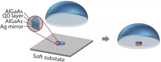
Figure1. (Color online) The dielectric antenna consisting of a QD-containing membrane, PMMA spacer, and the GaP solid immersion lens. Reproduced with permission from Ref. [9]. Copyright 2018, Springer Nature.
Their design can be used to improve the extraction efficiency of QDs for practical applications in any telecommunication network. The broadband antenna is also applicable to different optical-active materials. The efficient generation of entangled photon pairs in this report paves the way for the development of various quantum technologies.
References:
[1] Müller M, Bounouar S, J?ns K D, et al. On-demand generation of indistinguishable polarization-entangled photon pairs. Nat Photonics, 2014, 8, 224
[2] Dousse A, Suffczyński J, Beveratos A, et al. Ultrabright source of entangled photon pairs. Nature, 2010, 466, 217
[3] Claudon J, Bleuse J, Malik N S, et al. A highly efficient single-photon source based on a quantum dot in a photonic nanowire. Nat Photonics, 2010, 4, 174
[4] Kako S, Santori C, Hoshino K, et al. A gallium nitride single-photon source operating at 200 K. Nat Mater, 2006, 5, 887
[5] Zhao C, Chen Y H, Xu B, et al. Evolution of InAs nanostructures grown by droplet epitaxy. Appl Phys Lett, 2007, 91, 033112
[6] Zhao C, Chen Y H, Xu B, et al. Study of the wetting layer of InAs/GaAs nanorings grown by droplet epitaxy. Appl Phys Lett, 2008, 92, 063122
[7] Benson O, Santori C, Pelton M, et al. Regulated and entangled photons from a single quantum dot. Phys Rev Lett, 2000, 84, 2513
[8] Deshpande S, Heo J, Das A, et al. Electrically driven polarized single-photon emission from an InGaN quantum dot in a GaN nanowire. Nat Commun, 2013, 4, 1675
[9] Chen Y, Zopf M, Keil R, et al. Highly-efficient extraction of entangled photons from quantum dots using a broadband optical antenna. Nat Commun, 2018, 9, 2994
点击阅读赵超教授文章:
An efficient entangled-photon source from semiconductor quantum dots
Chao Zhao and Zhijie Wang
J. Semicond. 2020, 41(1), 010401
doi: 10.1088/1674-4926/41/1/010401
“王占国院士从事科研工作60周年”专刊
《半导体学报》组织了一期“王占国院士从事科研工作60周年”专刊,并邀请中国科学院半导体研究所王智杰研究员、德国亚琛工业大学赵超教授和德国莱布尼兹-汉诺威大学丁飞教授共同担任特约编辑。该专题已于2020年第1期正式出版并可在线阅读,欢迎关注。
专刊详情请见:半导体学报2020年第1期——王占国院士从事科研工作60周年专刊

(来源:半导体学报公众号)

